
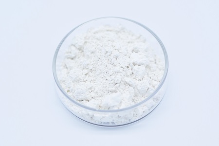
Raman spectra of tellurium dioxide single crystal
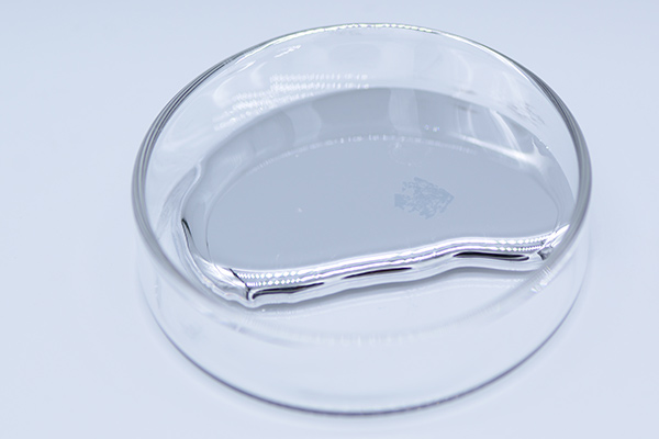
Tellurium dioxide single crystal has excellent acousto-optical properties which melting point is 733.8℃. There are three kinds of structures: one is the red-gold tetragonal crystal, the other is the plate titanium tetragonal crystal, and the third is the rutile deformed tetragonal crystal. The third structure is the only crystal that can be grown artificially, in which oxygen ions form a hexagonal, distorted octahedron, while tellurium ions enter the octahedron void. Each single crystal cell contains four molecules of TeO2 and three edges of each octahedron. Raman spectrum is one of the important methods to study the structure of matter. As early as 1970, Pine et al. in the UK measured the polarizing Raman spectra of TeO2 at temperatures of 85 and 295K. Compared with some similar oxides such as rutilite and alpha-quartz, its Raman spectrum peaks are very strong and sharp.Crystal growth mechanism is a problem that has been studied a lot in current crystal theory and paid much attention to by scientists. Because crystal growth is finally carried out on solid-liquid surface, the structure and behavior of solid-liquid interface play a decisive role in the growth mechanism.We conducted a study on the high-temperature Raman spectral characteristics of the solid/liquid boundary layer structure of TeO2 crystal growth by melt method, which will be helpful to better understand and study the microstructure of the crystal growth boundary layer, and provide an explanatory basis for the research on growth mechanism of functional crystal materials. The figure below shows the Raman spectrum of solid state of TeO2 crystal at room temperature of plane 001 and plane 110at room temperature, whereinmain spectral peak of its spectrum line is basically consistent with that of TeO2 T=300K.Based on group theory analysis, the spectral peaks at room temperature can be identified. In the figure, two spectral lines are clear and the spectral peaks are sharp. The strong peak at 648cm-1 is characteristic peak of the tetragonal crystal system. The spectral peaks below 200cm-1 are caused by relative vibration between octahedrons of TeO2 cells and the long range ordered lattice vibration. Spectral peaks of 200-800cm-1 correspond to the contraction and flexural vibrations of Te-O. The vibration modes of 200-800cm-1 on plane 001 and 110 were identified analytically (as shown in table 1 and table 2), and the spectral peaks of 200-800cm-1 on plane 001 had three vibration modes: Symmetric Te-O contraction, anti - symmetric Te-O contraction, angular bending in plane, four vibrating membranes in total.
 Hot words
 +86 731-8972336
 santech @santechchem.com
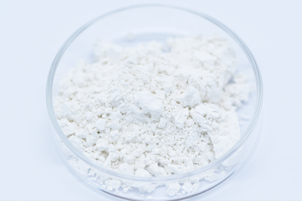

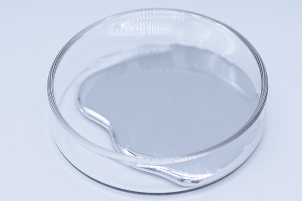
Tellurium dioxide single crystal has excellent acousto-optical properties which melting point is 733.8℃. There are three kinds of structures: one is the red-gold tetragonal crystal, the other is the plate titanium tetragonal crystal, and the third is the rutile deformed tetragonal crystal. The third structure is the only crystal that can be grown artificially, in which oxygen ions form a hexagonal, distorted octahedron, while tellurium ions enter the octahedron void. Each single crystal cell contains four molecules of TeO2 and three edges of each octahedron. Raman spectrum is one of the important methods to study the structure of matter. As early as 1970, Pine et al. in the UK measured the polarizing Raman spectra of TeO2 at temperatures of 85 and 295K. Compared with some similar oxides such as rutilite and alpha-quartz, its Raman spectrum peaks are very strong and sharp.Crystal growth mechanism is a problem that has been studied a lot in current crystal theory and paid much attention to by scientists. Because crystal growth is finally carried out on solid-liquid surface, the structure and behavior of solid-liquid interface play a decisive role in the growth mechanism.We conducted a study on the high-temperature Raman spectral characteristics of the solid/liquid boundary layer structure of TeO2 crystal growth by melt method, which will be helpful to better understand and study the microstructure of the crystal growth boundary layer, and provide an explanatory basis for the research on growth mechanism of functional crystal materials. The figure below shows the Raman spectrum of solid state of TeO2 crystal at room temperature of plane 001 and plane 110at room temperature, whereinmain spectral peak of its spectrum line is basically consistent with that of TeO2 T=300K.Based on group theory analysis, the spectral peaks at room temperature can be identified. In the figure, two spectral lines are clear and the spectral peaks are sharp. The strong peak at 648cm-1 is characteristic peak of the tetragonal crystal system. The spectral peaks below 200cm-1 are caused by relative vibration between octahedrons of TeO2 cells and the long range ordered lattice vibration. Spectral peaks of 200-800cm-1 correspond to the contraction and flexural vibrations of Te-O. The vibration modes of 200-800cm-1 on plane 001 and 110 were identified analytically (as shown in table 1 and table 2), and the spectral peaks of 200-800cm-1 on plane 001 had three vibration modes: Symmetric Te-O contraction, anti - symmetric Te-O contraction, angular bending in plane, four vibrating membranes in total.

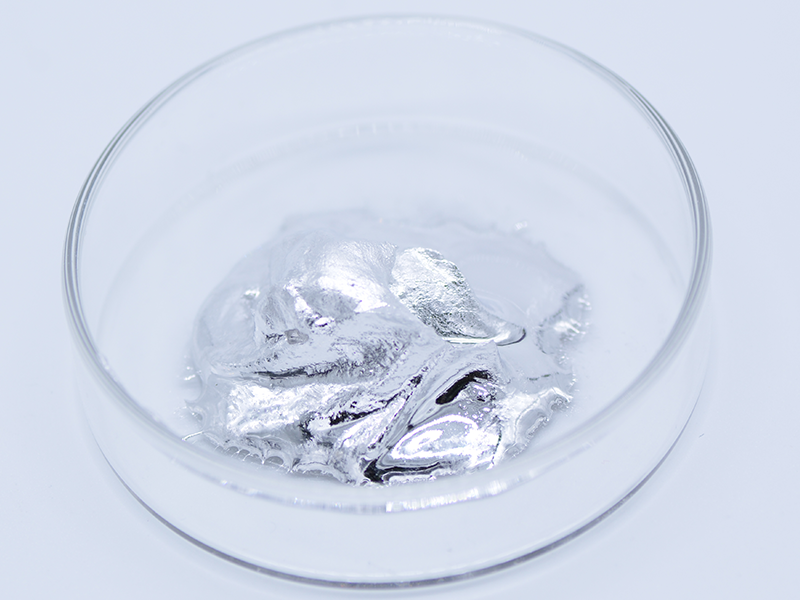
Gallium is a chemical element that has the symbol Ga and atomic number 31. A soft silvery metallic poor metal, gallium is a brittle solid at low temperatures but liquefies slightly above room temperature and will melt in the hand. It occurs in trace amounts in bauxite and zinc ores. An important application is in the compounds gallium nitride and gallium arsenide, used as a semiconductor, most notably in light-emitting diodes (LEDs).Elemental gallium is not found in nature, but it is easily obtained by smelting. Very pure gallium metal has a brilliant silvery color and its solid metal fractures conchoidally like glass. Gallium metal expands by 3.1 percent when it solidifies, and therefore storage in either glass or metal containers is avoided, due to the possibility of container rupture with freezing. Gallium shares the higher-density liquid state with only a few materials like germanium, bismuth, antimony and water.Gallium also attacks most other metals by diffusing into their metal lattice. Gallium for example diffuses into the grain boundaries of Al/Zn alloys or steel., making them very brittle. Also, gallium metal easily alloys with many metals,[citation needed] and was used in small quantities in the core of the first atomic bomb to help stabilize the plutonium crystal structure.The melting point temperature of 30°C allows the metal to be melted in one's hand. This metal has a strong tendency to supercool below its melting point/freezing point, thus necessitating seeding in order to solidify. Gallium is one of the metals (with caesium, rubidium, francium and mercury) which are liquid at or near normal room temperature, and can therefore be used in metal-in-glass high-temperature thermometers. It is also notable for having one of the largest liquid ranges for a metal, and (unlike mercury) for having a low vapor pressure at high temperatures. Unlike mercury, liquid gallium metal wets glass and skin, making it mechanically more difficult to handle (even though it is substantially less toxic and requires far fewer precautions). For this reason as well as the metal contamination problem and freezing-expansion problems noted above, samples of gallium metal are usually supplied in polyethylene packets within other containers.

Under standard conditions, Germanium is a brittle, silvery-white, semi-metallic element.This form constitutes an allotrope known as α-Germanium , which has a metallic luster and a diamond cubic crystal structure, the same as diamond. While in crystal form, Germanium has a displacement threshold energy ofAt pressures above 120 kbar, Germanium becomes the allotrope β-Germanium with the same structure as β-tin. Like silicon, Gallium, Bismuth, Antimony, and water, Germanium is one of the few substances that expands as it solidifies from the molten state.Germanium is a semiconductor. Zone refining techniques have led to the production of crystalline Germanium for semiconductors that has an impurity of only one part in 1010, making it one of the purest materials ever obtained.The first metallic material discovered (in 2005) to become a superconductor in the presence of an extremely strong electromagnetic field was an alloy of Germanium, uranium, and rhodium. Pure Germanium suffers from the forming of whiskers by spontaneous screw dislocations. If a whisker grows long enough to touch another part of the assembly or a metallic packaging, it can effectively shunt out a p-n junction. This is one of the primary reasons for the failure of old Germanium diodes and transistors.

Certain compounds of Indium, such as oxides, sulfides, and phosphates, are used in the manufacture of yellow and orange-yellow glass, as well as specialty optical glass. Indium borate glass containing barium or cadmium can absorb moderate-intensity X-rays and absorb higher neutrons than thermal neutrons.Halides of indium, such as indium iodide, are commonly used as additives in metal halide lamps to enhance the output power of the illumination and improve the quality of the spectrum.Indium ingot: trapezoidal, smooth surface, white with metallic luster, mainly used in the manufacture of various alloys, special welding, coating, electronics and production of high purity indium.Indium trioxide: light yellow, used in fluorescent screens, glass, ceramics, chemical reagents, etc.Indium hydroxide: used in batteries, glass, ceramic chemicals, etc.High-purity trimethyl indium: white crystalline crystal, mainly used as a raw material for epitaxial growth of indium-containing compounds and semiconductor photoelectric functional materials in the GAEHI process.High-purity indium chloride: colorless or white powder, mainly used in phosphor powder, III-V compound semiconductor, low-pressure nano lamp, manganese dry battery mercury-free negative electrode, (zinc) anti-corrosion additive, ITO transparent battery.Indium is a doping element in germanium transistors, and the largest amount of indium is used in the production of PNP germanium transistors.The amount of indium used in new applications is also increasing at a rate of 10%-20% per year.Because of its softer nature, it is also used for pressure cracking in some industries that require metal filling. Such as: vacuum gap filling material at higher temperatures.

Bismuth compounds are used as catalysts in the manufacturing process of synthetic fiber and rubber.When bismuth is combined with other metals such as lead, tin, iron and cadmium, it forms alloys with low melting points that can be used in fire detectors and extinguishers.Alloys of bismuth are also used in making sharp castings of objects subject to damage by high temperatures because the liquid metal expands 3.32 percent when it becomes solid.Bismanol, an alloy of bismuth and manganese, is a permanent magnet of high coercive force (a measure of magnetization) developed in the 1950s by the U.S. Naval Ordinance Laboratory in White Oak, Md. It was used in small motors. The bismuth metal is used as replacement for lead in shot and bullets. Bismuth can also be used in nuclear reactors and to make transuranium elements using a process called cold fusion.